Firmware Design for Periodically Waking STM32L1 Battery Nodes
Introduction
Battery life in a periodically waking microcontroller (MCU) is not a property of any single operating mode. It is the integral of current over time across a repeating cycle — a long stretch of deep sleep, a short transient where the device wakes and stabilizes its clocks, and a brief active burst where useful work happens before the device returns to sleep. Total consumed charge is the area under this current-vs-time curve, and battery life follows directly from it.
Framing the design this way is more useful than memorizing datasheet minima, because it makes the relative weight of each decision visible. A mode that draws 290 nA instead of 560 nA looks like a 2x improvement in isolation, but if the sleep floor already contributes a small fraction of per-cycle charge, halving it changes the area under the curve by almost nothing. The same framing also explains why a few microseconds of avoidable wake-up latency, repeated millions of times over a deployment, can outweigh the entire sleep-floor budget.
The STM32L1 family (Cortex-M3, "ultra-low-power" line) is a convenient reference because each segment of the waveform maps to a concrete, configurable feature: a hierarchy of sleep states with different wake-up latencies and leakage currents, a multi-speed internal RC oscillator that governs how fast the device comes back to life, and a real-time clock (RTC) that can survive the deepest retained-state mode to schedule the next wake event. The reasoning generalizes to the L0, L4, L5, and U5 ultra-low-power series, though the absolute current figures shift with each process generation.
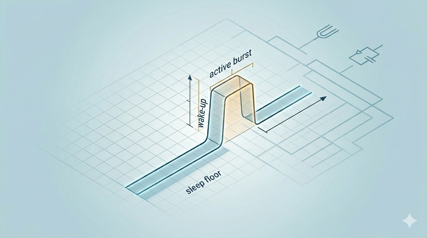
The Shape of One Wake Cycle
A single cycle of a periodically waking system has four distinguishable segments, in time order:
- Sleep floor — the long, flat, lowest-current segment. Duration is set by the wake-up interval; current is set by the chosen deep-sleep mode and what is left powered (RTC, brown-out reset, retained SRAM, GPIO leakage).
- Wake-up transient — a brief, current-intermediate ramp while the regulator returns to its run-mode operating point and the clock source restarts and stabilizes. Duration is the effective startup latency.
- Active burst — the high-current segment where the CPU and peripherals do useful work: sensor reads, computation, radio transmission.
- Re-entry — a short tail while firmware saves any state and reconfigures pins before re-entering sleep.
Each design lever discussed below changes the height or width of one of these segments. The objective is the smallest total area, not the lowest single point.
Shaping the Sleep Floor: Mode Depth and Hidden Leakage
The STM32L1 reference manual (RM0038) defines a descending sequence of sleep states. The two that matter for periodic wake-up are Stop and Standby, with representative figures from the STM32L152xE datasheet (3.0 V, 25 °C):
| Mode | State retained | Typical current | Effect on cycle |
|---|---|---|---|
| Stop (no RTC) | SRAM + registers | 560 nA | Lowest floor that still preserves working state |
| Stop + RTC | SRAM + registers + timekeeping | 1.4 µA | Adds scheduled wake-up at modest cost |
| Standby (no RTC) | Backup domain only | 290 nA | Lower floor, but wake = full reset |
| Standby + RTC | Backup domain + timekeeping | 1.11 µA | Lowest practical floor with scheduling |
For reference, Run mode draws roughly 195 µA/MHz, and the two intermediate active modes — Low-power run and Low-power sleep — sit at about 11 µA and 4.6 µA respectively. These figures vary by package, memory size, and silicon revision; the controlling number is always the current datasheet for the specific part, not a representative table.
The architecturally significant point is what each mode discards. Stop mode gates all clocks except the RTC/low-speed sources but keeps SRAM and register contents intact, so firmware resumes transparently. Standby mode powers down the core domain and clears SRAM (apart from a small backup-register block), so wake-up runs the reset vector — a separate "cold-start" code path that must reconstruct all working state from non-volatile memory. The 270 nA difference between Stop+RTC and Standby+RTC is rarely the deciding factor; the deciding factor is whether the firmware can tolerate losing SRAM every cycle.
A frequently underestimated contributor to the sleep floor is leakage outside the MCU's published mode current. Floating or pulled GPIO pins, sensor quiescent current, and regulator leakage can each exceed the MCU's nanoampere floor. Driving unused pins to a defined level or configuring them as analog inputs before sleep entry removes input-buffer leakage paths that would otherwise dominate a 290 nA budget. Below roughly 1 µA, the MCU is often no longer the largest term in the system, and continued effort on mode depth yields little.
Narrowing the Wake-Up Transient
Every wake-up transient is time spent at an intermediate current that produces no useful work, and it delays the start of the active burst. Several firmware decisions set its width.
On exit from Stop mode, the STM32L1 automatically reverts the system clock to the multi-speed internal (MSI) RC oscillator; it does not restore whatever clock tree was active before sleep. The hardware wake-up itself is fast — the datasheet quotes an 8 µs wake-up time. But if the application needs a higher frequency or an external high-speed crystal (HSE), the time to reconfigure and re-stabilize that source is part of the effective latency and must be counted, not assumed away.
Two further levers narrow the transient:
- Clock target on wake-up. Resuming directly on the MSI at a frequency adequate for the task avoids waiting for an HSE crystal to re-stabilize. Many periodic-sensing tasks complete comfortably within an MSI range and never need to spin up a high-speed source at all.
- Regulator setting versus latency. The Stop-mode low-power regulator option reduces sleep-floor current but lengthens the time to bring the core rail back to its run-mode operating point. The lowest-floor configuration is therefore not automatically the narrowest-transient one — a direct trade between two segments of the same waveform.
/* STM32L1 Stop-mode entry/exit (HAL-style) */
HAL_SuspendTick();   /* Stop the 1ms tick so it can't block Stop entry or wake early */

/* Low-power regulator lowers the sleep floor but widens the wake-up transient */
HAL_PWR_EnterSTOPMode(PWR_LOWPOWERREGULATOR_ON, PWR_STOPENTRY_WFI);

/* Resumes here on MSI at its reset-default range; no HSE has been restored */
SystemClock_Config();  /* Re-establish target clock tree only if the task needs it */
HAL_ResumeTick();
What the Active Burst Actually Costs: Peripherals Compared
Reducing the active-burst width only helps if the dominant current contributors during that burst are known. On the STM32L1, the core executing from flash sets the baseline at roughly 195 µA/MHz, but several peripherals add to it in very unequal proportions, and a few of them also extend the burst through their own startup times.
The analog front end dominates. The 12-bit successive-approximation (SAR) analog-to-digital converter (ADC) — the on-chip block that turns a sensor voltage into a number — draws on the order of a milliamp from the analog supply while converting, which is several times the core's own draw at a moderate clock. This makes the ADC, not the CPU, the largest single term in many sensor-node active bursts. The leverage is therefore in conversion duration, not core speed: enabling the ADC only immediately before the conversion and disabling it immediately after, converting the minimum number of channels, and avoiding unnecessarily long sampling times all shrink the highest part of the curve. Leaving the ADC clock-enabled between bursts is a common oversight that quietly inflates the sleep floor.
The voltage reference is a startup-time cost more than a current cost. The internal reference (VREFINT, a ~1.2 V bandgap used for calibration and supply monitoring) draws only tens of microamperes, but it has a non-trivial settling time, and on these parts it can be switched off in Stop mode together with the brown-out reset to save sleep-floor current. The design tension is that re-enabling it on each wake adds settling latency to the active burst. Note also that VREFINT is not directly usable as the ADC's reference — the ADC references VREF+/VDDA — so for ratiometric accuracy the relevant question is the stability of the analog supply rail, not VREFINT's own draw.
The PLL is rarely worth it for short bursts. The phase-locked loop (PLL, which multiplies a low input frequency up to a higher core clock) adds both a continuous current draw and a lock time of tens of microseconds before the clock is usable. For a burst that completes in a few milliseconds at a modest frequency, running directly from the MSI or HSI without engaging the PLL usually both lowers current and shortens the wake transient. The PLL earns its place only when the active task is compute-bound enough that the higher core frequency shortens the burst by more than the PLL's lock time and current overhead cost.
Timers and digital peripherals are individually small but additive. Each enabled peripheral on the AHB/APB buses adds dynamic current roughly proportional to its clock frequency; an individual timer, SPI, or USART is a single-digit-to-low-tens-of-µA/MHz contributor — minor next to the ADC. The significant effect is cumulative and persistence-related: peripheral clocks are gated individually through the RCC enable registers, and any peripheral left clock-enabled keeps drawing whether or not it is in use. Disabling peripheral clocks the burst does not need — and re-enabling only what the next burst requires — is generally higher-value than micro-optimizing any single peripheral's settings. The datasheet's per-peripheral current table gives the exact µA/MHz adders for ranking candidates.
I/O configuration is the cheapest sleep-floor lever. A GPIO left as a digital input with its Schmitt-trigger input buffer active will conduct a leakage current if the pin floats near the switching threshold — a path that can exceed the MCU's entire nanoampere sleep floor. Configuring unused pins as analog inputs disables that input buffer and removes the path; this is typically the single most effective action for reaching the datasheet sleep figures. Driven outputs are a separate, load-dependent cost: any pin sourcing or sinking current into an external load (an LED, a pull-up, a sensor enable line) adds that current directly, so returning such pins to a non-driving state before sleep matters as much as the MCU's own mode.
| Contributor | Relative active-burst impact | Also affects | Primary lever |
|---|---|---|---|
| ADC (converting) | High (~mA class) | — | Minimize conversion time; disable when idle |
| Core @ frequency | Baseline (~195 µA/MHz) | Burst width | Lowest frequency that meets the deadline |
| PLL | Moderate + lock-time | Wake transient | Avoid for short bursts; run on MSI/HSI |
| VREFINT / BOR | Low (~tens of µA) | Wake transient (settling) | Disable in Stop where accuracy allows |
| Individual timer/SPI/USART | Low (µA/MHz each) | — | Clock-gate when unused |
| Floating digital GPIO | Leakage (can exceed sleep floor) | Sleep floor | Set unused pins to analog input |
/* Set unused GPIO pins to analog input before sleep:
 * disables the input Schmitt-trigger buffer and removes the
 * floating-input leakage path that otherwise dominates the sleep floor */
GPIO_InitTypeDef g = {0};
g.Pin  = GPIO_PIN_All;          /* All pins on the port not used by the application */
g.Mode = GPIO_MODE_ANALOG;      /* Analog mode = input buffer off, no pull resistors */
g.Pull = GPIO_NOPULL;
HAL_GPIO_Init(GPIOx, &g);

/* Gate the clock to peripherals the next burst does not need.
 * A clock-enabled peripheral keeps drawing even when idle. */
__HAL_RCC_ADC1_CLK_DISABLE();   /* Re-enable immediately before the next conversion */
__HAL_RCC_TIM2_CLK_DISABLE();
The practical ordering that falls out: chase ADC conversion time and peripheral clock-gating first (largest active-burst terms), confirm I/O is in an analog/non-driving state second (largest avoidable sleep-floor term), and treat PLL avoidance as both a current and a latency win for short bursts. Micro-optimizing an individual timer or shaving the last few microamperes off VREFINT is worthwhile only after those larger terms are settled.
The Clock-Source Decision: When RC Is Enough
The wake-up schedule is driven by the RTC, and the RTC's clock source is the central accuracy-versus-cost decision.
The STM32L1 offers a low-speed internal RC oscillator (LSI), nominally around 37 kHz, that can clock the RTC with no external components. Two properties make it a poor timekeeper: its frequency is not a clean binary divisor of 1 Hz, and it drifts by a few percent across temperature and supply voltage. The low-speed external crystal (LSE) at 32.768 kHz is the conventional alternative — 32768 = 2^15 divides cleanly to a 1 Hz tick, and crystal accuracy is on the order of tens of parts per million.
The decision reduces to whether wake-up occurrence is sufficient or wake-up timing must track real elapsed time:
- LSI is sufficient when the interval tolerance is loose — "sample roughly once a minute," where a few percent of drift has no functional consequence and no external system depends on the device's timestamps. This saves bill-of-materials cost, board area, and the small continuous current of the crystal and its load capacitors.
- The LSE crystal is justified once accumulated drift would visibly desynchronize the device — calendar-aligned logging, coordinated multi-node wake windows in a sensor network, or any server-side schedule the device must meet. Over months, the difference is between seconds of drift (LSE) and minutes (LSI).
A middle path worth noting: the STM32L1 can hardware-trim the MSI against an accurate reference, and where an LSE is already present, the MSI can be auto-calibrated against it. This lets the system clock inherit crystal-grade accuracy without running a separate high-speed crystal — useful when a communication peripheral needs accuracy but the board cannot afford a second oscillator.
/* RTC clock source — the accuracy/cost decision in code */
RCC_OscInitTypeDef osc = {0};

/* Loose-interval applications: LSI, no external crystal */
osc.OscillatorType = RCC_OSCILLATORTYPE_LSI;
osc.LSIState       = RCC_LSI_ON;
/* PeriphClkInit.RTCClockSelection = RCC_RTCCLKSOURCE_LSI; */

/* Timing-critical applications: LSE 32.768 kHz, tens of ppm */
osc.OscillatorType = RCC_OSCILLATORTYPE_LSE;
osc.LSEState       = RCC_LSE_ON;
/* PeriphClkInit.RTCClockSelection = RCC_RTCCLKSOURCE_LSE; */
Risks and Limitations of LSI: Where "Good Enough" Stops
The case for LSI rests entirely on the wake-up interval being the only timing requirement. The moment a peripheral needs a frequency-accurate clock, LSI is disqualified — not marginally, but by a wide margin.
LSI for UART baud-rate generation does not provide adequate accuracy. An asynchronous UART link tolerates only a limited cumulative clock mismatch between its two endpoints. With 16x oversampling (the receiver samples each bit period sixteen times and uses the middle samples) and a standard 8N1 frame, the theoretical ceiling is around ±5% — half a bit accumulated over ten bit-times — but the practical budget receivers are specified against is roughly ±2% cumulative across both ends, which is why a conservative design keeps each side under ±1%. An uncalibrated LSI cannot meet this: its ~37 kHz nominal frequency is not a clean divisor of standard baud rates, and its tolerance alone exceeds the entire budget. In practice LSI is not even routed as the clock for a conventional USART; the realistic "internal RC for UART" option is the high-speed internal RC (HSI), and even HSI's ±1% room-temperature figure consumes most of the budget by itself, leaving little margin for the far end.
Temperature range is the constraint that is easiest to overlook. RC-oscillator accuracy specs such as HSI's ±1% are quoted at 25 °C. Frequency drifts with both temperature and supply voltage, so error grows as conditions move away from the trim point. A consequence is that an internal-RC UART link which works correctly on the bench can begin dropping frames at the edges of an industrial range (−40 °C to +85 °C or +105 °C), where accumulated drift pushes the mismatch past the receiver budget. LSI is worse on every axis — uncalibrated to start, with large drift across the full range — so it offers no usable temperature window for any baud-rate-critical function.
The defensible rule: an internal RC source for UART is acceptable only over a narrow band near 25 °C with generous baud-rate margin, while LSI is never appropriate for UART or any other frequency-accurate peripheral at any temperature. Where the active burst must drive a UART reliably across temperature, the design needs a crystal — an LSE (which can additionally auto-trim the MSI to crystal-grade accuracy on the STM32L1) or an HSE.
| Clock source | RTC / periodic wake | UART baud generation | Accuracy vs temperature |
|---|---|---|---|
| LSI (~37 kHz RC) | Acceptable only for loose intervals | No — far exceeds budget | Large drift across full range |
| HSI (16 MHz RC) | N/A (not an RTC source) | Marginal; narrow temp band only | ±1% at 25 °C, degrading at extremes |
| LSE (32.768 kHz crystal) | Yes — tens of ppm | N/A directly, but enables MSI auto-trim | Stable, tens of ppm |
| HSE (crystal) | N/A | Yes | Stable across range |
Calculating the Area Under the Curve
Average current is the time-weighted sum of the segments:
I_avg = (I_sleep·t_sleep + I_wake·t_wake + I_active·t_active) / T_period
Worked example: a node wakes every 30 s from Stop+RTC (1.4 µA), spends ~10 µs in the wake-up transient (~1.5 mA average during ramp), then 3 ms of active work over SPI at ~4 mA, and returns to sleep.
| Segment | Current | Duration | Charge |
|---|---|---|---|
| Sleep floor | 1.4 µA | ≈ 29.997 s | ≈ 42.0 µA·s |
| Wake-up transient | ~1.5 mA | 10 µs | ≈ 0.015 µA·s |
| Active burst | 4 mA | 3 ms | 12.0 µA·s |
| Period | — | 30 s | ≈ 54 µA·s |
I_avg = 54 µA·s / 30 s ≈ 1.8 µA
The sleep floor and the active burst contribute comparable charge here, even though the active current is roughly 3,000x higher — because charge is current times time, and the time axis is dominated by sleep. The lever with the most leverage depends on which term is larger: shorten the active burst or lengthen the interval when the active term dominates; deepen the sleep mode and reduce external leakage when the floor dominates (typically only at multi-minute-plus intervals). Chasing the last nanoamperes of mode current is rarely the highest-value move at second-scale intervals.
Battery Life Estimation
Converting an average-current figure to battery life is a direct division, with the caveat that primary-battery capacity (in milliamp-hours, mAh) is itself rate- and temperature-dependent, and datasheet capacity is typically measured under continuous low-rate discharge rather than the pulsed load a periodic wake-up pattern produces.
Estimated life (hours) ≈ Battery capacity (mAh) / I_avg (mA)
For the 1.8 µA average above against a typical 220 mAh CR2032-class cell, the computed life exceeds the cell's self-discharge and shelf-life floor by a wide margin — a reminder that once I_avg reaches the low microamperes, battery self-discharge (a few percent per year for a good primary lithium cell) and shelf life, rather than the active-discharge calculation, govern the deployment lifetime.
Conclusion / Summary
Treating the design as one current-vs-time waveform reorders the priorities sensibly: optimize whichever segment contributes the most area, and stop optimizing a segment once it is no longer the dominant term. Stop+RTC is the reasonable default for second-to-minute intervals needing transparent state retention; Standby+RTC earns its place when intervals are long and firmware is built around persisting state to non-volatile memory each cycle. Within the active burst, the ADC conversion time and any un-gated peripheral clocks are usually the largest terms, the PLL is best avoided for short bursts, and unused I/O placed in analog mode is the cheapest route to the datasheet sleep floor. The LSI-clocked RTC is adequate whenever timing tolerance is loose; the LSE crystal is warranted once drift would desynchronize the device from wall-clock time or from peers, and any frequency-accurate peripheral such as a UART across temperature requires a crystal rather than an internal RC.
This framing applies to sleep-dominated duty cycles — periodic sensing, logging, beaconing. It is the wrong tool for near-continuous workloads (motor control, streaming, always-on links), where run-mode efficiency and dynamic voltage/frequency scaling, not sleep-state selection, set the energy budget.
References / Further Reading
[1] STMicroelectronics, "STM32L151xE / STM32L152xE — Datasheet," DS10002.
[2] STMicroelectronics, "RM0038: STM32L100xx, STM32L151xx, STM32L152xx and STM32L162xx advanced Arm-based 32-bit MCUs — Reference manual."
[3] STMicroelectronics, "AN3300: How to calibrate an STM32L1xx internal RC oscillator," Application Note.
[4] Analog Devices, "Determining Clock Accuracy Requirements for UART Communications," Technical Article.
[5] STMicroelectronics, "AN2867: Oscillator design guide for STM8AF/AL/S, STM32 MCUs and MPUs," Application Note.
