Raspberry Pi Pico (RP2040) Architecture: A Dual-Core MCU with Programmable I/O
Raspberry Pi Pico (RP2040) Architecture: A Dual-Core MCU with Programmable I/O
Introduction
The RP2040, launched in early 2021 on the USD 4 Raspberry Pi Pico board, was notable for two reasons: it was the first chip designed by Raspberry Pi rather than sourced from an existing vendor, and it priced a dual-core 32-bit microcontroller at roughly a dollar in volume. By 2024 it had become a fixture in maker, education, and a growing range of commercial embedded designs, supported by a mature C/C++ SDK, MicroPython, and CircuitPython.
For an embedded engineer, the relevant question is not the price headline but the architectural choices behind it. The RP2040 makes an unusual set of trade-offs: a modest CPU paired with generous SRAM, no on-die non-volatile memory, and a programmable I/O fabric that substitutes for the fixed-function serial peripherals a conventional MCU would multiply. Understanding where those choices help and where they constrain a design is the basis for deciding whether the part fits a given application.
Core architecture
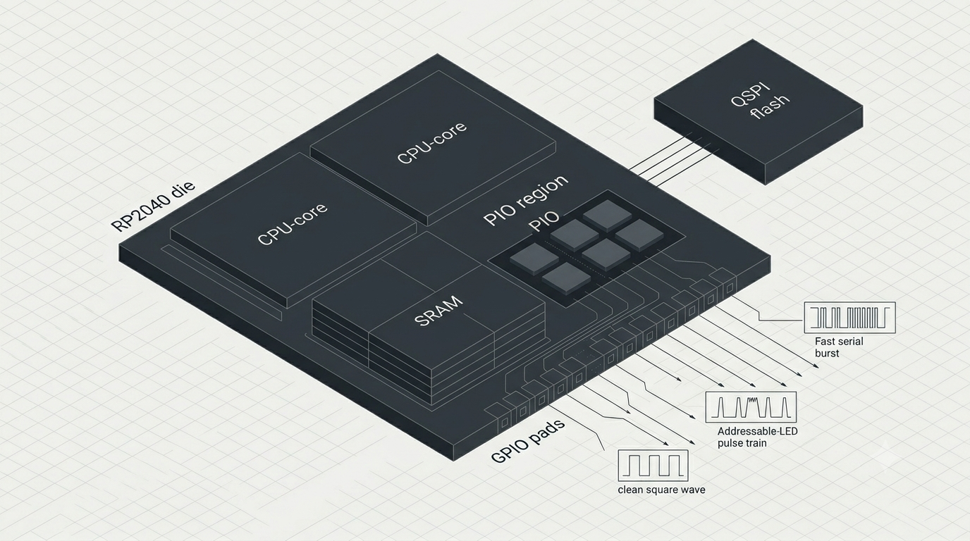
The RP2040 is built around two Arm Cortex-M0+ cores running at a nominal maximum of 133 MHz (the device is widely run higher via the on-chip PLLs, but 133 MHz is the specified figure). The Cortex-M0+ implements the ARMv6-M architecture: a small, low-power core with a reduced instruction set, no floating-point unit, and no DSP extensions.
Key architectural elements as of 2024:
- Dual symmetric Cortex-M0+ cores with a shared bus fabric.
- 264 KB on-chip SRAM arranged in six independent banks, allowing the two cores and the DMA engine to access different banks concurrently without contention.
- No internal flash. Code is stored in external QSPI flash and executed in place (XIP) through a dedicated cache. This is the single most consequential architectural decision.
- 30 multifunction GPIO (26 exposed on the Pico board), of which four are shared with the ADC.
- Fixed-function peripherals: 2x UART, 2x SPI, 2x I2C, 16 PWM channels, a USB 1.1 host/device controller, and a 12-bit SAR ADC with five input channels (four external plus an internal temperature sensor).
- 12-channel DMA controller for moving data between memory, peripherals, and the PIO FIFOs without CPU involvement.
- SIO (Single-cycle I/O) block: a tightly coupled set of resources outside the normal bus, including fast GPIO access, 32 hardware spinlocks, a pair of inter-core FIFOs, two integer dividers, and two interpolators.
- 8x PIO state machines (two PIO blocks of four state machines each) — covered in detail below.
- Boot ROM implementing the UF2 USB mass-storage bootloader, which lets the device appear as a drive for drag-and-drop programming.
The split between a deliberately simple CPU and a rich set of data-movement and I/O resources (DMA, SIO, PIO) is the defining characteristic. Work that would burden the CPU on a conventional part is offloaded to these blocks.
What the RP2040 introduced
Three things distinguished the part at introduction and remained relevant through 2024:
- The PIO subsystem, which has no direct equivalent on mainstream Cortex-M competitors. It allows a designer to create new I/O interfaces in firmware rather than being limited to the fixed peripherals on the die.
- A cost/SRAM balance atypical for the price tier: 264 KB of SRAM is large for a sub-dollar MCU, and it enables frame buffers, audio buffers, and PIO-driven data streaming that a smaller memory could not hold.
- External-flash architecture with XIP caching, which decouples code size from the silicon. A designer chooses flash capacity at board level (commonly 2–16 MB), rather than selecting an MCU SKU by flash size.
The Programmable I/O (PIO) subsystem
The PIO is the architectural feature that most justifies considering the RP2040. It consists of two PIO blocks; each contains four independent state machines and a shared instruction memory of 32 slots. Each state machine is a tiny, deterministic processor purpose-built for shifting bits in and out of pins with cycle-accurate timing.
Per state machine, the resources are:
- Two shift registers — Output Shift Register (OSR) and Input Shift Register (ISR) — with configurable shift direction and automatic push/pull thresholds.
- Two scratch registers, X and Y, used as counters and temporaries.
- A 4-word TX FIFO and a 4-word RX FIFO, which can be joined into a single 8-word FIFO in one direction.
- A fractional clock divider (16.8 fixed-point) deriving the state-machine clock from the system clock.
- Side-set capability, allowing a pin to be driven in parallel with the main instruction (useful for generating clock lines).
The instruction set is just nine instructions — JMP, WAIT, IN, OUT, PUSH, PULL, MOV, IRQ, and SET — most executing in a single cycle. Despite this minimalism, the combination of autopush/autopull, the FIFOs, DMA feeding those FIFOs, and precise timing lets a state machine implement protocols at speeds the CPU could never bit-bang reliably.
A short PIO program illustrates the model — a square-wave generator that toggles a pin using side-set:
.program squarewave
    set pindirs, 1       ; set the mapped pin as output (runs once at start)
loop:
    set pins, 1 [1]      ; drive pin high, then delay 1 extra cycle
    set pins, 0 [1]      ; drive pin low, then delay 1 extra cycle
    jmp loop             ; repeat forever, fully independent of the CPU
The output frequency is determined entirely by the state-machine clock divider, so it is jitter-free regardless of CPU load. This deterministic timing, replicated across eight state machines, is the heart of the PIO's value.
In practice, PIO is used to synthesize interfaces that the fixed peripherals do not provide, including: WS2812/NeoPixel addressable LED timing, additional UART/SPI/I2C channels beyond the two hardware instances, quadrature encoder decoding, DPI/VGA and even DVI video output, SD-card interfaces, stepper-motor pulse generation, and — because the RP2040 lacks a CAN controller — bit-banged CAN. The pattern is consistent: where a design needs an unusual interface or simply more of a common one, PIO provides it without external logic.
Advantages
- Cost. Among the lowest-priced dual-core 32-bit MCUs, with the Pico board at roughly USD 4.
- PIO flexibility. Custom and additional I/O interfaces in firmware, with deterministic timing and DMA integration.
- Large, banked SRAM. 264 KB enables buffering-heavy applications and reduces external-RAM pressure.
- Dual core with clean inter-core primitives. Hardware spinlocks and inter-core FIFOs make a producer/consumer split between the two cores straightforward.
- Strong tooling and documentation. A well-documented C/C++ SDK, MicroPython, and CircuitPython, with an extensively detailed datasheet and the RP2040 Hardware Design guidance.
- Simple programming workflow. The UF2 mass-storage bootloader requires no external programmer for basic use.
Disadvantages
- Modest CPU. The Cortex-M0+ (ARMv6-M) has no FPU and no DSP instructions, limiting floating-point and signal-processing throughput. Hardware integer dividers and interpolators in the SIO partially compensate, but heavy math is slow relative to Cortex-M4/M7 parts.
- No internal flash. External QSPI flash adds a component and a board-level dependency; although XIP caching mitigates the latency, code execution from external memory is not free of penalty on cache misses.
- Limited atomic support. ARMv6-M lacks exclusive load/store (LDREX/STREX); concurrency relies on the hardware spinlocks rather than standard atomic instructions.
- Few fixed peripherals. Only two each of UART, SPI, and I2C, and no dedicated CAN or Ethernet MAC. PIO compensates but consumes development effort and state-machine resources.
- ADC limitations. The 12-bit SAR ADC has documented nonlinearity (DNL) characteristics that constrain precision measurement.
- Minimal security. No TrustZone and limited secure-boot facilities in this generation, which restricts use in security-sensitive products.
Where the RP2040 is a compelling choice
The architecture favors specific design profiles:
- Cost-sensitive, I/O-diverse designs that need several non-standard or duplicated interfaces, where PIO replaces external glue logic or a larger MCU.
- Deterministic I/O offload, such as LED matrices, motor pulse trains, or custom serial links, where PIO handles timing-critical work while the CPU runs application logic.
- Buffer-heavy applications — simple audio, small displays, data logging — that benefit from the large SRAM and DMA.
- Education and rapid prototyping, given the tooling, low cost, and drag-and-drop programming.
It is a weaker fit where the workload is dominated by floating-point or DSP computation, where on-die flash and a single-chip BOM are required, where hardware CAN/Ethernet or strong security features are mandatory, or where a large number of simultaneous high-precision analog channels is needed.
Conclusion
The RP2040 is best understood as a deliberate rebalancing of the conventional microcontroller: a simple, inexpensive dual Cortex-M0+ paired with unusually large SRAM, external XIP flash, and a programmable I/O fabric that turns I/O definition into a firmware task. The PIO subsystem is the decisive feature — eight deterministic state machines that synthesize interfaces the fixed peripherals omit, integrated with DMA for high-throughput streaming.
Choose the RP2040 when a design is cost-constrained, needs flexible or additional I/O, and can use the PIO to offload timing-critical work, or when generous SRAM and a strong software ecosystem matter. Avoid it when the application is compute- or DSP-heavy, requires single-chip flash, depends on hardware CAN/Ethernet or robust security, or needs high-precision analog acquisition. Within its intended envelope the part is distinctive; outside it, a conventional Cortex-M4/M7 with integrated flash and richer peripherals remains the better engineering choice.
References / Further Reading
- Raspberry Pi Ltd. RP2040 Datasheet — A microcontroller by Raspberry Pi. Raspberry Pi Ltd.
- Raspberry Pi Ltd. Raspberry Pi Pico C/C++ SDK. Raspberry Pi Ltd.
- Raspberry Pi Ltd. Hardware Design with RP2040. Raspberry Pi Ltd.
- Arm Limited. Cortex-M0+ Technical Reference Manual (ARMv6-M architecture). Arm Developer Documentation.
