Programming the RP2040 PIO: From WS2812 to Motor Drive — and Where Only PIO Will Do
Introduction
The prior post identified the PIO as the RP2040's defining feature and listed the interfaces it can synthesize. That list answers what PIO can do; it does not explain how the subsystem achieves deterministic, multi-megabit I/O on a 133 MHz Cortex-M0+ that has no DSP extensions and no clock cycles to spare for bit-banging.
The gap between fixed-function peripherals and a general-purpose CPU is where PIO operates. A fixed peripheral (a hardware UART or SPI block) is fast and offloads the CPU completely, but its protocol is frozen in silicon and its instances are few. CPU bit-banging is infinitely flexible but pays for that flexibility with jitter, interrupt latency, and full core occupancy; above a few megahertz it stops being reliable, and at high line rates it stops being possible. PIO occupies the middle: eight small, deterministic processors that run independently of the CPU, feed and drain through DMA, and can be reprogrammed at the firmware level.
This post treats PIO as a programmable peripheral generator rather than a curiosity. The objective is to give an engineer enough of the execution model to estimate, for a given interface, whether PIO is the right tool — and to recognize the cases where it is the only tool available on a part in this class.
The reference point: what "conventional MCU" means here
To make the comparisons concrete, the baseline throughout this post is the STM32F family, the most common general-purpose Cortex-M line in the RP2040's price and integration tier:
- STM32F0 / STM32F1 (Cortex-M0 / M3) are the closest peers on price. The STM32F103 in particular is the canonical low-cost workhorse.
- STM32F4 (Cortex-M4F) is the richer-peripheral reference: it adds an FPU, more timers, and more communication blocks, and is the part an engineer often reaches for when the RP2040's fixed peripherals fall short.
Two structural differences matter for the comparisons that follow. First, STM32F parts integrate flash on-die, whereas the RP2040 executes from external QSPI flash. Second — and more relevant to PIO — a typical STM32F carries several peripherals the RP2040 simply omits: a CAN controller (bxCAN on most F1/F4), an SDIO controller (F1/F4), timer encoder mode for quadrature decoding, and advanced-control timers (TIM1/TIM8) with complementary outputs and hardware dead-time. The RP2040 has none of these as fixed silicon. This is the framing for the rest of the post: PIO does three distinct jobs — it recovers peripherals the STM32F has but the RP2040 lacks, it multiplies instances of common peripherals, and it enables a handful of interfaces neither class provides in hardware.
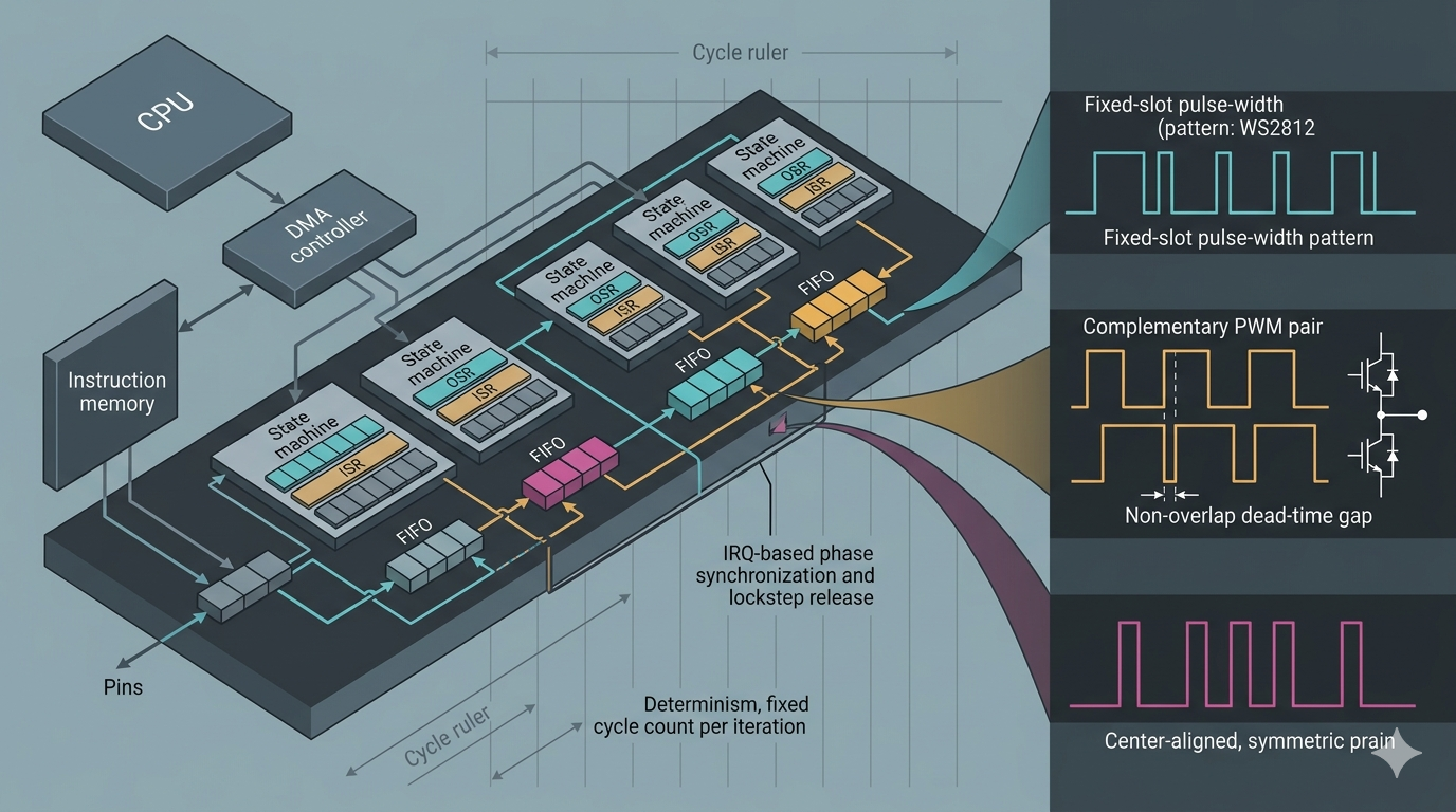
The PIO execution model
Each PIO block contains four state machines (SMs) and one shared instruction memory of 32 slots. All four SMs in a block execute from that same 32-instruction pool but maintain independent program counters, registers, clock dividers, and pin mappings. Two blocks give eight SMs and 64 total instruction slots.
A single SM exposes a deliberately small resource set:
- OSR / ISR — Output and Input Shift Registers, each with a configurable shift direction and an autopull/autopush threshold (1–32 bits).
- X / Y — two 32-bit scratch registers, used as counters and temporaries. The only arithmetic available is decrement-and-branch (
jmp x--) and comparison; there is no add, multiply, or divide. - TX / RX FIFOs — four words deep each, joinable into a single eight-word FIFO in one direction when the SM is unidirectional.
- Fractional clock divider — 16 integer + 8 fractional bits, deriving the SM clock from the system clock down to very low rates with sub-cycle resolution.
- Side-set / delay — a 5-bit field per instruction, split between driving up to five "side-set" pins in parallel with the instruction and inserting 0–31 idle cycles.
The instruction set is nine opcodes (JMP, WAIT, IN, OUT, PUSH, PULL, MOV, IRQ, SET), each executing in one SM cycle unless it stalls. Determinism comes from this: an SM program has a fixed, calculable cycle count per iteration, so the output timing is a function of the clock divider alone and is immune to CPU load, interrupts, or bus contention.
Two features turn this from a bit-banger into a streaming engine. Autopull refills the OSR from the TX FIFO automatically when it empties past the threshold, and autopush moves the ISR to the RX FIFO automatically when it fills — both without an explicit PULL/PUSH in the loop. Combined with DMA pacing, where each SM's FIFO raises a DREQ (data request) that gates a DMA channel, the data path becomes: memory → DMA → TX FIFO → OSR → pins (and the reverse for input), with the CPU touching none of it after setup.
Worked example 1: WS2812 timing with offload
WS2812 addressable LEDs encode bits as pulse widths on a single ~800 kHz line, with roughly ±150 ns timing tolerance. The canonical PIO driver uses side-set to carry the line state and structures every bit as a fixed 10-cycle slot:
.program ws2812
.side_set 1                       ; the one side-set pin carries the data line
.wrap_target
bitloop:
    out x, 1        side 0 [2]    ; shift next bit from OSR; hold line low (T3)
    jmp !x do_zero  side 1 [1]    ; go high; branch on a 0 bit (T1)
do_one:
    jmp  bitloop    side 1 [4]    ; 1 bit: stay high longer, then wrap (T2)
do_zero:
    nop             side 0 [4]    ; 0 bit: return low early, pad the slot (T2)
.wrap
With autopull set to 24 bits and the SM clock at 8 MHz, each bit occupies exactly 10 cycles = 1.25 µs. The CPU's only job is to point a DMA channel at the framebuffer and the SM's TX FIFO; DMA streams pixel words on the FIFO DREQ, and the timing never varies regardless of what either core is doing. A CPU bit-bang of the same protocol requires disabling interrupts for the duration of the frame and still risks violating the timing window on any stall. An STM32F has no native WS2812 peripheral either; the common workaround there is a timer-plus-DMA scheme driving the PWM compare register, which works but is rigid and consumes a timer.
Worked example 2: deterministic capture
Input is symmetric to output. A logic-capture SM samples a group of pins every cycle and relies on autopush to batch samples into the FIFO:
.program capture8
.wrap_target
    in pins, 8        ; sample 8 input pins into ISR each SM cycle
.wrap                 ; autopush (threshold 32) packs 4 samples per FIFO word
Set the SM clock to the desired sample rate, join the RX FIFO to eight words for input-only operation, and run a DMA channel paced by the RX DREQ into a RAM ring buffer. The result is a sampling front end with a constant sample interval — no interrupt jitter, no missed samples under load. This is the basis of the PIO-based logic analyzers that capture at tens of megasamples per second. A CPU sampling loop cannot guarantee the interval because any interrupt perturbs it; for arbitrary-width parallel capture at an arbitrary clock there is no general fixed peripheral, though some STM32F4 parts offer a constrained alternative through the DCMI camera interface or timer-paced DMA from the GPIO input register.
Worked example 3: counted pulse trains
The jmp x-- idiom turns an SM into a hardware counter, which is useful for generating an exact number of pulses — a step count for a stepper driver, for instance — pulled from the FIFO so a DMA channel can stream a motion profile:
.program npulses
.side_set 1
    pull             side 0       ; fetch pulse count N from the TX FIFO
    out  x, 32       side 0       ; load N into the X loop counter
count:
    nop              side 1 [3]   ; STEP pin high for 4 cycles
    jmp  x-- count   side 0 [3]   ; STEP low 4 cycles; decrement X; loop while X != 0
Because N arrives through the FIFO, a DMA channel can feed a sequence of segment counts, and the SM emits each segment with cycle-exact spacing. Acceleration ramps become a table in RAM rather than a tight, jitter-prone CPU timer ISR. The same pattern generates exact-length clock bursts, calibration pulses, or framing sequences.
Worked example 4: synchronizing multiple state machines
The IRQ instruction sets or clears one of eight PIO interrupt flags that any SM (in either block) can wait on. This provides lockstep coordination without CPU intervention — for example, releasing several output SMs on the same cycle so multi-channel signals stay phase-aligned:
; "master" SM, after all SMs are configured and stalled at their wait:
    irq set 4              ; raise flag 4

; each "slave" SM begins with:
    wait 1 irq 4           ; block here until flag 4 is set, then run in lockstep
The flags also serve as a lightweight producer/consumer handshake between SMs — one SM signals "byte ready," another waits on it — which is how a parallel bus or a multi-lane interface is split across several SMs that must stay synchronized.
Worked example 5: complementary, center-aligned PWM for motor drive
Motor control is the case that most sharply exposes the RP2040's PWM limits. Driving a half-bridge (a high-side and a low-side switch feeding one motor phase) requires complementary outputs — when one switch conducts, the other must not — separated by a dead-time: a short interval where both are off at every transition. Without it, both switches conduct briefly during the cross-over and short the DC rail (shoot-through). Field-oriented and BLDC drives additionally prefer center-aligned (symmetric) PWM, because centering the pulse in the period lowers the switching-harmonic content and aligns naturally with mid-period ADC current sampling.
On an STM32F this is dedicated silicon: the advanced-control timers TIM1/TIM8 generate complementary outputs (OCx / OCxN) with a programmable dead-time generator, center-aligned counting modes, and a hardware break input that shuts the outputs down within nanoseconds on a fault. The RP2040's PWM block has none of this — its slices produce two independent channels but no complementary pairing and no hardware dead-time. So on the RP2040 the choice is to carefully offset a pair of PWM channels or to synthesize the behavior in PIO, where the dead-time band is explicit in the instruction stream:
.program complementary_pwm
.side_set 2                 ; side-set drives {HS, LS}: 0b10 = HS on, 0b01 = LS on, 0b00 = both off
.wrap_target
    pull noblock            ; refresh conduction count each period; keep previous if FIFO empty
    out  x, 32              ; X <- conduction cycles for this period (CPU/DMA precomputes the value)
    nop            side 0b00 [DT]   ; rising-edge dead-time: both switches off DT+1 cycles
    mov  y, x      side 0b10        ; high-side on, low-side off
hi: jmp  y-- hi    side 0b10        ; hold high-side conduction for the loaded count
    nop            side 0b00 [DT]   ; falling-edge dead-time: both off again before LS turns on
    mov  y, x      side 0b01        ; low-side on, high-side off (symmetric count -> centered)
lo: jmp  y-- lo    side 0b01        ; hold low-side conduction
.wrap                               ; next period
Side-set carries the two gate-drive lines, the nop … [DT] instructions insert a guaranteed dead-time band of DT+1 cycles on both edges, and jmp y-- counts out each conduction phase. Equal high- and low-side counts give a symmetric, center-aligned waveform; an arbitrary duty cycle uses two distinct counts and the CPU precomputes them. A DMA channel feeding the TX FIFO then streams a per-period duty profile, exactly as in Example 3, and three of these SMs synchronized by an IRQ flag (Example 4) drive a three-phase bridge phase-aligned.
This example is also where the honest limit shows. PIO can reproduce the complementary/dead-time waveform, but it cannot replicate the STM32 break input's hardware fault shutdown: a PIO SM has no asynchronous "kill the outputs now" path, so a hardware over-current event must be handled with external gate-driver logic or by clamping the pins through another mechanism. For safety-critical drives, that pushes the design back toward a part with a dedicated motor-control timer.
Design trade-offs and limits
PIO is not unconstrained, and the limits are concrete:
- Instruction budget. 32 slots per block, shared by four SMs. A complex protocol can consume most of a block by itself, leaving the other three SMs starved. Programs that approach this limit force a choice between protocol complexity and SM count.
- No arithmetic. Only decrement, shift, compare, and move exist. Anything requiring addition, multiplication, CRC computation, or scaling must be precomputed in RAM, handled by the SIO's hardware divider/interpolators, or done on the CPU. PIO moves and times bits; it does not compute on them.
- Shallow FIFOs. Four words (eight when joined) sets a tight DMA-latency budget at high line rates. Sustained multi-megabit streams depend on keeping DMA serviced; FIFO underrun or overrun shows up as protocol errors, not graceful degradation.
- Limited branching and state. Two scratch registers and conditional jumps are the entire control-flow toolkit. State-heavy protocols are awkward and often split across SMs coordinated by IRQ flags.
- No asynchronous fault path. As Example 5 shows, PIO has no hardware equivalent of an advanced-timer break input; fast fault shutdown must come from outside the SM.
The practical method is to budget cycles per bit, multiply by line rate to get the required SM clock, confirm it is achievable from the system clock through the divider, and verify the FIFO depth gives DMA enough slack. If those numbers close, PIO works deterministically; if they do not, the interface belongs on a faster part or dedicated silicon.
When PIO solves the problem — and when only PIO can
The table below contrasts non-trivial I/O tasks across three implementation strategies: the fixed peripherals of an STM32F-class MCU, a pure CPU bit-bang on the RP2040, and PIO on the RP2040. The relevant distinction is not merely "easier" versus "harder" but whether a strategy is feasible at all on a part of this class.
| Task | Fixed peripheral on STM32F-class MCU | Pure CPU bit-bang (RP2040) | PIO (RP2040) |
|---|---|---|---|
| WS2812 strings (800 kHz, ±150 ns) | No native peripheral; timer+DMA on a PWM compare works but is rigid | Feasible only with interrupts disabled; violates timing under load | Native, DMA-fed, jitter-free; up to eight independent channels |
| DVI/HDMI output (≈252 Mbps TMDS) | Not available on this class (F4 has no TMDS; F7/H7 LTDC is parallel RGB only) | Not feasible — far exceeds achievable bit-bang rate | Feasible: PicoDVI serializes TMDS across overclocked SMs + DMA |
| Complementary center-aligned PWM + dead-time | Native and superior: TIM1/TIM8 give complementary outputs, hardware dead-time, break input | Possible at low PWM frequency; dead-time jitter risks shoot-through | Synthesized via two-pin side-set + counted dead-time band; no hardware break/fault path |
| 4–8 additional UARTs | Up to ~6 USART/UART on mid-tier STM32F4 | Feasible at low baud; jitters and scales poorly with channel count | Each SM = one full UART, DMA-fed; up to 8 channels |
| Quadrature encoder, high count rate | Native: TIM encoder mode decodes in hardware | GPIO-interrupt counting misses counts at high transition rates | SM tracks transitions deterministically; recovers what RP2040 lacks |
| Constant-rate parallel logic capture | Partial: timer-paced DMA from GPIO, or DCMI on some F4 (limited width/format) | Jitters; consumes a full core; drops samples on interrupt | Deterministic sample clock, autopush, DMA to RAM ring |
| CAN 2.0 | Native on most F1/F4 (bxCAN) | Impractical — arbitration and bit timing too demanding | Feasible with dedicated TX/RX SMs (community PIO-CAN); recovers a missing peripheral |
| SD 4-bit SDIO | Native: SDIO controller on F1/F4 | Cannot meet 4-bit timing at speed | Feasible: 4-bit SDIO synthesized in PIO; recovers a missing peripheral |
| Coordinated multi-channel phase-aligned pulses | Advanced timers with master/slave synchronization | Jitter under load; ties up a core for timing | DMA-driven profiles, phase-aligned via IRQ flags |
The pattern is consistent. Against the STM32F baseline, PIO does three different things. It recovers peripherals the STM32F has in silicon but the RP2040 omits — CAN, SDIO, encoder decoding, and the complementary/dead-time PWM behavior of advanced-control timers. It multiplies common peripherals beyond the RP2040's two hardware instances, as with the extra UARTs. And it is genuinely enabling for tasks neither class provides natively — clean WS2812 timing, DVI output, and arbitrary constant-rate parallel capture — that a CPU on this part cannot perform reliably or at all. The PWM row is the deliberate counterexample: there the STM32F's dedicated hardware is the better engineering answer, and PIO is the RP2040's recovery of a capability it lacks rather than an advantage over the conventional part.
Conclusion
PIO's value is not that it bit-bangs, but that it removes the two failure modes of bit-banging — jitter and core occupancy — while keeping the flexibility. The execution model is small and learnable: nine instructions, two shift registers, two counters, fractional clocking, and a side-set/delay field, made productive by autopush/autopull and DMA pacing. The shown fragments (WS2812 timing, deterministic capture, counted pulse trains, complementary motor PWM, and IRQ-flag synchronization) cover most of the idioms an engineer needs to reason about a new interface.
Use PIO when an interface is missing from the RP2040's fixed peripheral set, when more instances of a common interface are needed, or when timing-critical I/O must run independently of CPU load — and especially when the line rate or determinism requirement places the task outside what a CPU bit-bang can meet. Avoid leaning on PIO when the protocol requires real arithmetic per bit (CRC, scaling), when the program will not fit the 32-slot budget alongside the other SMs it must share with, when the FIFO depth cannot absorb the DMA latency at the target rate, or — as the PWM case shows — when a conventional MCU already provides the function in dedicated, fault-protected hardware. Measured against an STM32F-class part, the RP2040 with PIO trades fixed peripherals for a programmable I/O fabric: a clear win where that fabric fills a gap or enables the otherwise-impossible, and a deliberate compromise where the conventional silicon was already the right tool.
References / Further Reading
[1] Raspberry Pi Ltd., RP2040 Datasheet, "Chapter 3: PIO" and "Chapter 4.5: PWM," 2021 (revised through 2023). [Online].
[2] Raspberry Pi Ltd., Raspberry Pi Pico C/C++ SDK, "PIO" reference and pioasm documentation, 2021–2024. [Online].
[3] STMicroelectronics, RM0008 / RM0090 Reference Manuals (STM32F1 / STM32F4), advanced-control timer (TIM1/TIM8) and bxCAN/SDIO chapters, rev. through 2023. [Online].
[4] Raspberry Pi Ltd., pico-examples repository — PIO examples (ws2812, quadrature_encoder, logic_analyser, uart_tx/uart_rx, pio_blink), 2021–2024. [Online].
[5] L. Wren, PicoDVI: bit-banged DVI output from the RP2040, 2021. [Online].
[6] V. H. Adams, "Raspberry Pi Pico PIO," Cornell University ECE 4760 course notes, 2023. [Online].
