Building a Complete Power System Around the BQ25792 for a Jetson-Class Board
Introduction
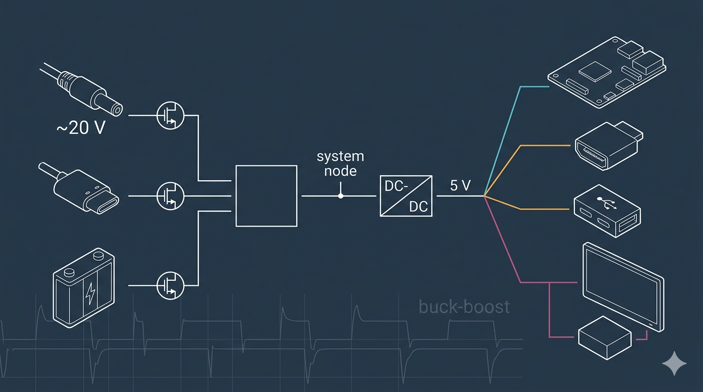
A compute module such as the Jetson Nano presents an awkward power profile for portable design: it requires a tightly regulated supply (the developer kit needs 5 V and tolerates brownout only to about 4.75 V, with no input regulation on the carrier board), yet system draw ranges from a few watts up to roughly 20 W. Adding a battery, a DC adapter, and a USB Type-C input — any of which may be the only source present — turns a single-rail task into a multi-source one. And in practice the module is rarely alone on the board: HDMI, a USB hub, a display, a fan, sensors, and level shifters all draw from rails the carrier must generate. The central difficulty is therefore twofold: reconciling a charger's native output with a load that needs a fixed rail, and budgeting the additional rails the surrounding peripherals require. The BQ25792 solves a large part of the first problem; the rest of the design is what turns one charger into a complete power system.
The core problem: an NVDC charger does not produce the system rail
The BQ25792 uses narrow voltage DC (NVDC) power-path management — an architecture that regulates the system node slightly above the battery voltage and never lets it fall below a configurable minimum, so the system keeps running even with a deeply discharged or absent battery. This is valuable for instant-on behaviour and for surviving battery swaps without a reset. The consequence is that the system rail tracks the battery: for a single cell it sits near 3.5–4.5 V, for a two-cell pack near 6–8.4 V. Neither is 5 V. The Jetson's strict 5 V requirement therefore cannot be met by the charger's system output directly; a dedicated regulation stage between the charger and the board is mandatory. This reframes the architecture cleanly: the charger manages the battery and source side, while one or more converters manage the load side.
Inside the BQ25792
The device integrates what would otherwise be a discrete buck-boost design:
- Buck-boost topology, 1–4 series cells, up to 5 A charge current, with all four power switches and the battery FET integrated, accepting 3.6–24 V at the input and charging correctly whether the input is above or below the pack voltage.
- Power-path / NVDC management, supplying the load directly from the adapter when present and from the battery (supplement mode) when the load exceeds the source rating.
- Input regulation loops — input voltage and input current dynamic power management (VINDPM, IINDPM) plus an Input Current Optimizer (ICO) that probes how much current an unknown source can deliver without collapsing it.
- Legacy fast-charge detection via D+/D- handshake (high-voltage dedicated charging port, HVDCP) and BC1.2 adapter detection.
- On-the-go (OTG) output, reversing the converter to source an adjustable 2.8–22 V on the input pin for downstream USB devices.
- A 16-bit analog-to-digital converter (ADC) for monitoring voltages, currents, and die temperature, plus I2C control and an autonomous, host-free charging mode.
Where it fits, and where it does not
The BQ25792 suits a battery-plus-adapter system in the single-digit-to-low-tens-of-watts range, where a 5 A integrated-FET charger in a 4 mm QFN gives a small bill of materials and good efficiency. It is well matched to a 2S or 3S pack feeding a downstream regulator.
It is less appropriate in several cases. It does not negotiate USB Type-C Power Delivery contracts — the D+/D- HVDCP handshake is a legacy mechanism, not Type-C communication on the CC lines — so a separate controller is needed for anything above the default 5 V/15 W from a Type-C source. The 5 A figure is a charge-current ceiling in an integrated-FET package; sustained high system current plus charging concentrates heat in a small die, so beyond roughly 60–75 W a controller driving external MOSFETs scales better. It tracks input voltage rather than performing true maximum power point tracking (MPPT, the perturb-and-observe loop a solar panel needs), so photovoltaic input is a poor fit. And it tops out at four series cells.
Alternatives
| Device | Topology / FETs | Distinguishing trait | Best-fit case |
|---|---|---|---|
| BQ25792 | Buck-boost, integrated, 5 A | Dual-input mux, OTG, compact | Battery + adapter, ≤ ~tens of W |
| BQ25798 | Buck-boost, integrated, 5 A | Adds true VOC-based MPPT and a fast backup mode | Solar / energy-harvesting input |
| BQ25790 | Buck-boost, integrated, 5 A | Same core in a smaller wafer-level package | Space-critical handhelds |
| BQ25703A | Buck-boost controller, external FETs | Scales to higher power; PROCHOT host-throttle line | Higher-power systems beyond a 5 A integrated part |
The BQ25798 is the closest sibling: the same charging core with genuine MPPT and a backup mode that holds up the load directly from the battery on source loss — justified only when solar input or that fast switchover is actually needed. The BQ25703A trades integration for headroom, which makes sense when continuous system power exceeds what an integrated 5 A part dissipates comfortably.
The DC input stage for a ~20 V adapter
A laptop-class brick (commonly 19–20 V) is a convenient high-power DC source, and 20 V sits inside the charger's 3.6–24 V operating window. The practical issues are at the margins, and they matter.
Headroom to the limits. A 20 V steady-state input leaves only a few volts to the 24 V operating ceiling, and the absolute-maximum rating sits above that with finite margin. Hot-plugging a brick into a connector with bulk input capacitance excites an LC resonance between the cable/lead inductance and that capacitance, and the input node can overshoot well past the steady-state voltage. A transient-voltage-suppression (TVS) clamp — a diode that conducts hard above a chosen voltage — placed at the jack and rated to clamp below the absolute maximum is the standard defence, together with adequate bulk capacitance and a controlled turn-on of the input switch to limit inrush. A mis-plugged higher-voltage adapter is a related risk; an input over-voltage cut-off (either the charger's own input OVP or an external OVP load switch) keeps a 24 V-plus source from reaching the converter.
Input regulation and source qualification. When a source appears, the charger measures the open-circuit input voltage and sets its VINDPM threshold a fixed offset below it (roughly 1.4 V below for sources at or above 7 V). For a 20 V brick this lands the threshold near 18.6 V, so as the load rises the charger backs off current before it can drag the adapter down — the input simply rides along its regulation point instead of collapsing. The charger also runs a poor-source check: it briefly loads the input and, if the voltage sags below a threshold, marks the source invalid, parks the input in a high-impedance state, and retries periodically. The design consequence is concrete: an undersized or high-impedance adapter is rejected rather than browned-out, so the adapter must be rated for the full system-plus-charge current, and the programmed input current limit should reflect the brick's real rating.
Source selection and the external FETs. The charger's dual-input selector does not switch the high-current path itself; it drives gate signals (ACDRV) to external back-to-back MOSFET pairs — an "ACFET–RBFET" arrangement — on each input. The ACFET passes current when the input is selected; the reverse-blocking RBFET prevents the battery or the other source from back-feeding an unpowered or lower-voltage adapter. This is why simple diode-OR'ing is avoided: two sources of different stiffness (a hard 20 V brick versus a current-limited port) cannot share or hand off load cleanly through diodes. These FETs carry the full input current in both charge and discharge directions, so their voltage rating must exceed the input (a 30 V-class part for a 20 V brick) and their on-resistance must be low — TI's own evaluation board uses 60 A-class devices, and higher FET resistance lengthens the charge-current taper near full charge. The selector's gate drive also slews the FET on gradually, which doubles as the inrush-control mechanism.
Filtering, fusing, and bias. Because the charger is a switching converter, the DC input benefits from an input EMI filter (a small pi filter or common-mode choke) to keep switching ripple off the adapter lead, plus a fuse sized above the worst-case input current. Reverse-polarity protection on a barrel jack (an ideal-diode controller or a series P-FET) guards against a wrong-polarity plug. One easily missed detail: the charger's internal bias regulator may be unavailable in a battery-only condition, so the interrupt line's pull-up rail is best taken from an always-present 1.8 V or 3.3 V supply rather than from that internal regulator.
Beyond the module: the carrier-board power tree
Powering the Jetson module is only the largest line item. A working carrier board fans the 5 V system rail out into several domains, and each peripheral interface has its own expectation. The table below is a representative rail tree for a Nano-class board.
| Rail | Typical source | Principal loads |
|---|---|---|
| 5 V main (≥ 4–6 A) | Buck/buck-boost from the NVDC SYS node | Compute module, USB port VBUS, HDMI +5 V pin, fan |
| 3.3 V | Buck or LDO from 5 V | USB hub controller, level shifters, microSD, sensors, display logic, I2C pull-ups |
| 1.8 V | LDO/buck from 3.3 V or 5 V | Camera (CSI) I/O, eMMC, some sensors |
| Backlight (≈ 9–25 V) | Boost LED driver from 5 V | LCD backlight LED string (constant-current) |
| 2.8 V / 1.2 V (optional) | Small LDOs | Camera analog and core rails |
A few interfaces deserve specific attention because their requirements are easy to under-provision.
HDMI. The video itself comes from the SoC's display output, but the HDMI connector has a dedicated +5 V power pin that the source side must drive; the standard requires the source to supply a minimum on the order of 55 mA on that pin so the sink can power its hot-plug-detect and read its identification data (EDID) even when otherwise unpowered. This is a small but non-optional 5 V load, and an ESD-protected, current-limited feed to that pin is good practice.
On-board USB hub and downstream ports. A hub controller is a logic device — it typically runs from 3.3 V (some parts also need a 1.2 V core, usually from an internal regulator) and handles only data. The port power is separate: each downstream Type-A port draws its VBUS from the 5 V rail through a current-limited load switch (a "power-distribution switch") with a fault flag, sized per the port class — 500 mA for a USB 2.0 high-power port, 900 mA for USB 3.x, and up to 1.5 A for a BC1.2 charging port. A four-port hub can therefore add several amps of potential 5 V load on its own, which is frequently the dominant term in the budget after the module.
LCD / display. A display splits into two power problems. The panel logic and interface (MIPI DSI or parallel RGB) usually want 3.3 V, sometimes with a 1.8 V I/O rail and panel-specific analog supplies. The backlight is the larger consumer: a series string of LEDs driven at constant current by a boost converter that steps the 5 V rail up to the string voltage, commonly somewhere in the 9–25 V range depending on LED count. Brightness control is by the driver's dimming input rather than by varying the rail. Treating the backlight as a simple resistive 5 V load is a common under-estimate.
Logic domains and the rest. The 3.3 V rail also feeds level shifters (the Nano's 40-pin header signals pass through 3.3 V translators), the microSD interface (3.3 V, with 1.8 V for the high-speed UHS-I mode), I2C pull-ups, and most sensors. A camera over the CSI interface adds small 1.8 V/2.8 V/1.2 V analog and core rails from dedicated LDOs. None of these is large individually, but collectively they justify a properly sized 3.3 V buck rather than a single hot LDO.
Why the tree loops back to the front end. The total 5 V load — module peak plus hub ports plus HDMI plus backlight plus fan — can realistically reach 4–6 A, i.e. 20–30 W at the rail. That power is drawn from the battery through the charger's power path: at a 2S pack (~7.4 V) a 25 W system load is roughly 3.4 A from the cells before adding charge current, and all of it passes through the selection FETs and the charger. The downstream budget therefore sets the FET sizing, the charger's continuous-current headroom, and the minimum adapter and USB-PD contract needed to both run the board and charge at a useful rate. The peripheral rails are not a separate problem from the charger choice; they define it.
Control and configuration
Even though autonomous charging works, full performance comes from configuring the charger over I2C, typically from a small MCU or the PD controller:
// BQ25792 minimal init over I2C (host = MCU or PD controller).
// Register offsets and field encodings per datasheet Rev. C register map.
bq_write(REG_CHG_VOLTAGE, mv_to_code(8400)); // 2S target: 4.20 V/cell fast-charge limit
bq_write(REG_CHG_CURRENT, ma_to_code(2000)); // charge current within pack and thermal limits
bq_write(REG_INPUT_ILIM, ma_to_code(3000));  // cap draw to the brick / negotiated source rating
bq_write(REG_MIN_SYS_V,  mv_to_code(6000));  // NVDC floor: keep SYS above post-reg dropout
bq_write(REG_CTRL_ICO,   ICO_ENABLE);        // probe unknown-source capability automatically
bq_write(REG_ADC_CTRL,   ADC_ENABLE);        // enable monitoring of V/I/temperature
// Cell count and default switching frequency are set by the PROG-pin resistor at power-on.
Setting the input current limit to the source's real rating is the link between the input stage and the charger: the limit caps the draw so neither a 20 V brick nor a USB-PD contract is overloaded, and supplement mode draws the shortfall from the battery.
Conclusion
The BQ25792 is a strong default for the charging and source-management half of a battery-powered compute board: it consolidates a buck-boost charger, power path, input regulation, and multi-source handling into one part, and its NVDC behaviour keeps the system alive across battery faults and swaps. It is the right choice when the pack is 1–4 cells, the budget is single-digit-to-low-tens of watts, and the input is an adapter or USB source rather than a solar panel. It is incomplete or wrong when the design needs true MPPT (the BQ25798 fits), when sustained power exceeds what a 5 A integrated-FET part dissipates (a controller such as the BQ25703A scales further), or when Type-C profiles above 5 V are required, since the charger performs no Type-C negotiation on its own.
Two architectural points carry the design. First, a power-path charger is not a system regulator: the NVDC node tracks the battery, so a dedicated 5 V post-regulator sized for peak load is mandatory. Second — and this is where many designs are under-scoped — the module is not the whole load. A real carrier board needs a small tree of rails: 5 V for the module, USB VBUS, the HDMI power pin, and the fan; 3.3 V for the hub controller, level shifters, storage, and display logic; 1.8 V for camera and storage I/O; and a boost-driven backlight rail for the LCD. For a ~20 V adapter the input stage needs TVS clamping below the absolute maximum, over-voltage cut-off, reverse-blocking selection FETs rated above the input, an EMI filter, and an input current limit matched to the brick. Designing the rail tree and the input protection as first-class parts of the deliverable — not afterthoughts to the charger selection — is what produces a system that runs reliably from any of its three sources while charging.
References
- Texas Instruments, BQ25792 I2C Controlled, 1-4 Cell, 5-A Buck-Boost Battery Charger with Dual-Input Selector and USB PD 3.0 OTG Output, datasheet SLUSDG1 (Rev. C), 2022.
- Texas Instruments, BQ25792EVM, BQ25798EVM and BQ25798BKUPEVM User's Guide (schematic, BOM, and register setup).
- Texas Instruments, bq25703A I2C Multi-Chemistry Battery Buck-Boost Charge Controller with System Power Monitor and Processor Hot Monitor, datasheet (Rev. A).
- NVIDIA Corporation, Jetson Nano Developer Kit User Guide and "Power Supply Considerations for Jetson Nano Developer Kit," developer.nvidia.com.
- USB Implementers Forum, USB Power Delivery Specification, Revision 3.x, usb.org.
